

Let’s discuss some components you’ll have to know pretty damn well if you’re going to build one of these. Don’t be intimidated by the names here: it’s like Daru adding “FG204 ver. 2.37” to the end of everything.
2.1 Bit Shift Register: The SN74HC595
The SN74HC595 is an 8-bit, serial-in, parallel shift-out register that holds the 4-bit binary values representing the digit on the Nixie tube. This device is capable of transmitting a numerical input over a serial connection into a physical manifestation of the represented number, opening and closing eight gates that directly represent the bits of the binary number. This device will be employed in conjunction with the K155ID1.
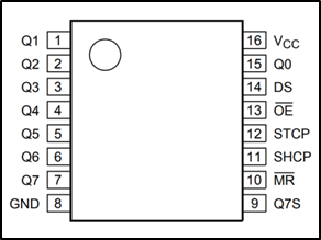
| Pin | Description |
| Vcc | Power pin |
| GND | Ground |
| DS / Serial | Serial input. |
| Output enable (active when LOW) | |
| STCP / RCLK | Storage register clock pin |
| SHCP / SRCLK | Shift register clock pin |
| MR | Master reset (active when LOW) |
| Shift register clear | |
| QA- QH | Bits 1-8, LSB to MSB |
| QH’ | Daisy chain out (to next Serial connec.) |
What’s important to observe is that the bits transferred into the shift register through Serial first enter the QA register, then are procedurally shifted towards the QH. Therefore, when we interface with this device, the LSB will end up being the last shifted value, housed in QA, and conversely, the MSB will house the first shifted value (in QH). Any further bit shifts will result in the QH bit being shifted to the next shift register, into its QA space.
Our end goal is to drive the nixie tubes. The K155ID1 chip, which will be discussed next, is the component that allows the 4-bit binary number to be converted into a signal that drives one number at a time. By daisy-chaining three of the SN74HC595 chips together, we have six available 4-bit binary numbers to drive our six nixie tubes. We use the Serial, RCLK and SRCLK to drive this process.
The STCP pin is the storage register clock pin. When it is low, the device “starts listening” for binary values to be introduced through the Serial line. When we change it to high, the device stops listening, then shifts the input data to the output line.
The SHCP pin is the shift register clock pin. The most important characteristic of this pin is its behavior on a rising edge transition — when it changes from low to high, all the values in our shift register are shifted by one place. QA is shifted to QB, QB to QC, and so on. The value in QH is shifted through the QH‘ pin, which connects to the next register’s Serial line, entering it into its QA position.
The Serial pin holds the data transferred from the microcontroller: a single bit, zero or one, low or high. The value in this register is shifted in when the SHCP pin undergoes a rising edge transition.
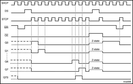
We observe this interaction in the above timing diagram table, adapted from a Nexperia datasheet [3]. The SHCP and STCP line share a relationship of one-half phase off from each other, as their behavior is contingent upon the rising-edge transition. When the DS (or Serial) pin receives a high signal, the SHCP pin receives a rising-edge signal from low to high, and the SHCP pin is low, the device processes the signal from the DS line and places it in the first register (QA). When the STCPline transitions to high, it transitions the input data to the output line and “stops listening” for new values.
The interplay between the STCP and SHCP line continues; each rising-edge transition of the SHCP pin drives the original signal from the DS pin one step further along the registers. Eventually, this signal reaches the Q7s or QH’ line, and if the QH’ line is daisy-chained to the next SN74HC595 DS line, that value is placed in its first register position.
TL;DR — This thing is gonna let us push the numbers we want to see into the Nixie Tubes from the microcontroller.
2.2 The Binary-to-BCD Chip: K155ID1
The K155ID1 (known to Russians as the К155ИД4, or the SN74155N) is a binary-to-BCD driver that converts our 4-bit nybble of binary numbers into a signal for the correct digit on our Nixie tubes.
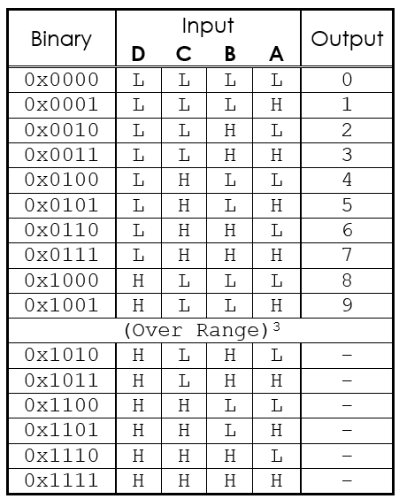
We observe on the pinout schematic that the values 0-9 are represented. For this particular chip (that only represents values 0-9), any value greater than 9 (or 0x0110, binary ten) results in no output. For convenience, we can use these values as “dead outputs” when we don’t want to display a number.
A specialized feature about this chip is that it is directly intended for use with high-voltage Nixie tubes (after all, the documentation contains a Russian document from the cold war era). The Logic Diagram shows us that Zener diodes and PNP BJT logic is present in the device. Since BJTs are present, the signal obtained from our microcontroller is segregated from the high-voltage connection to the Nixie tubes running in excess of 200 volts. The segregation of these two voltage lines ideally prohibits corruption of the STM32 microcontroller, which runs on a standard input of 5 volts, which is exactly the same as the voltage provided over a Serial line.
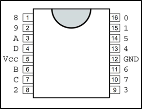
The figure above displays the pinouts of the K155ID1 chip for quick reference. The pins marked A, B, C, and D represent the four input bytes. According to the logic of Table 2.3, the 4-bit input corresponds to the numerical outputs displayed. These ten output lines, numbered 0 through 9, are directly connected to the cathode wires of the Nixie Tube. The Vcc line allows the bipolar junction transistors in the integrated circuit to “switch” between inputs.
TL;DR With the input from the first chip, this one sets the Nixie Tubes to show the correct number.
Here’s a truth table I’ve adapted to explain.
2.3 Using Both These IC’s Together
This graphic I made summarizes he whole process of what we’re doing here:
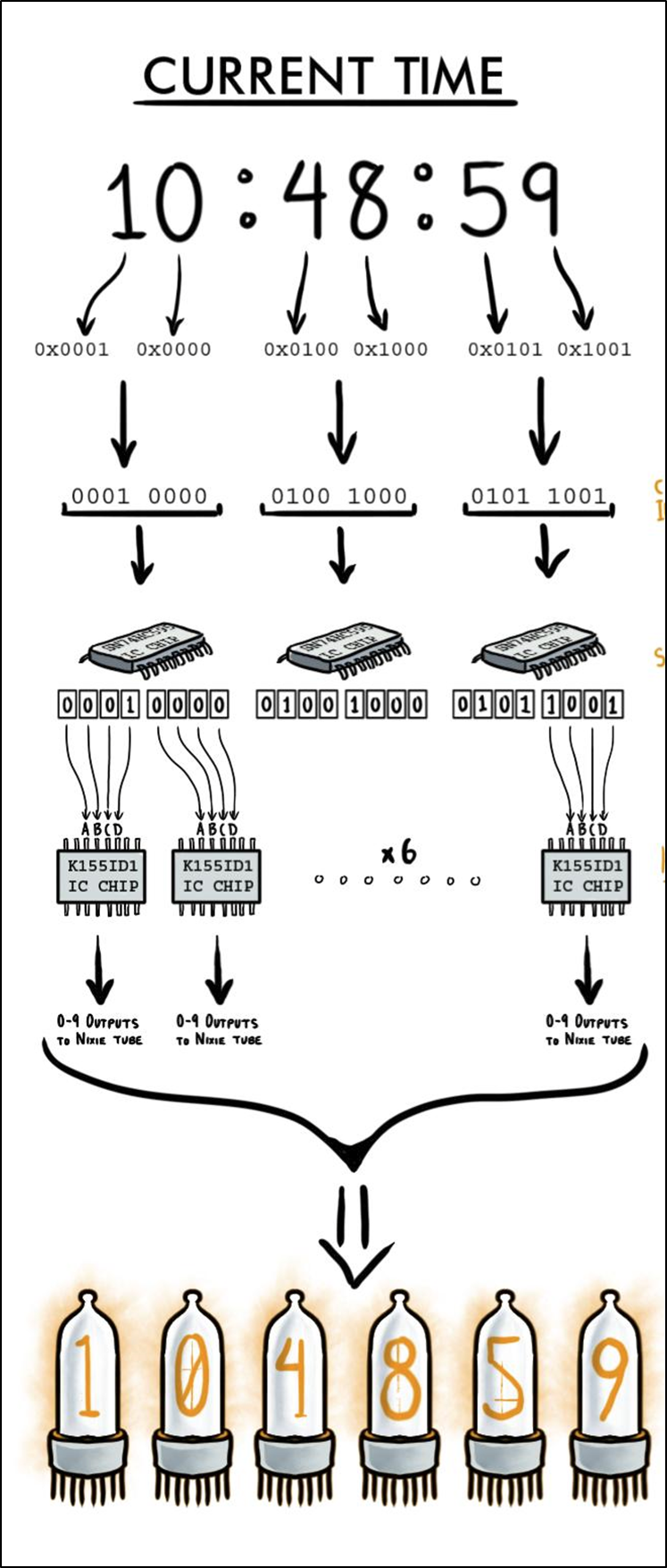
Properly interfacing with the Nixie tubes requires us to understand how the two ICs communicate.
Although further programming description will take place in Section 4, Figure 2.4 illustrates the procedure used to transition binary values into numbers on the clock:
- The numerical time is calculated through use of the C++ program.
- Each ones- and tens-place digit is separated and stored into individual values, and then converted to binary.
- Binary pairs are concatenated into 8-bit bytes for transference to the SN74HC595 chip using the shift operator.
- The bit-shift operation takes place, shifting all three bytes into place in the SN74HC595 chip.
- The information in the most significant nybble and least significant nybble are transferred to the K155ID1 chip. Each of these contain a 4-bit binary number representing the digit to display on the Nixie tube.
- The high voltage signal through the anode of the Nixie tube is open on all cathode lines, except for the desired number, causing the requested number to glow.
Further description of the wiring diagram will be provided in the third post (Circuit Schematics), and program code for interfacing with both of these devices will be provided in the fourth post.
2.3 The Brains: ESP32 Featherboard (Adafruit)

The Adafruit ESP-32 Huzzah microcontroller is an excellent featherboard for prototyping purposes. To save time constructing the Nixie tube clock, using a featherboard prevents us from soldering thermal ground planes and using a heat gun to solder intricate components. Take, for example, the USB-to-UART chip already present on the ESP32 feather —— with terminals nearly as small as the width of a human hair, this process requires specialized equipment beyond the budget of a simple hobbyist. In an effort save time, effort, and frustration, the featherboard is employed in this design. In addition to this, its power equates well with the requirements of the project: with four distinct timer channels, a sufficient number of additional GPIO pins, and low power requirements and power consumption, this makes the ESP32 an excellent choice [5].
Using Sloeber, an IDE built off of the Arduino workspace that packs a lot more power, we can interface with the ESP-32 quickly to prototype code.
Voltage Step-Up: The NCH6100HV
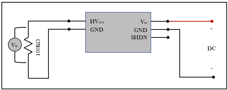
The NCH6100HV, designed by Yan Zeyuan, supplies us with the voltage required to drive the Nixie tubes. This step-up converter accepts a 12V signal and amplifies it to 200V, supplying the filament with enough power to ionize the neon gas.
An important calibration is required to accurately step the voltage up to 200 volts. On the circuit board there is a potentiometer that increases the high voltage output with respect to the clockwise rotation angle. From the starting orientation shown in the figure below, my module required at least a 270-degree rotation to break 200 volts.
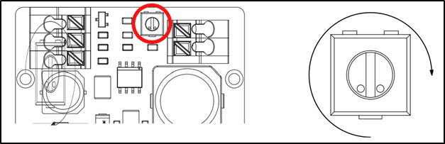
The test shown in the next image allows us to determine the correct calibration, as some devices may differ depending on the voltage. For a standard 12V input, specified by the Bill Of Materials in the first post, we can simulate this voltage by using a DC power supply and setting up a simple circuit to test this. Both GND terminals of the NCH6100HV are connected to their respective ground and voltage lines; the input to the positive and negative leads of the DC power supply, and the high voltage ground-and-power to the rest of the circuit.
Iteratively turn the potentiometer half a quarter-turn at a time. Warning—— For safety purposes, each time ensure total deactivation of the input voltage line: turn off the DC power supply and disconnect both leads before adjusting the potentiometer with a screwdriver. Read and understand the disclaimer before proceeding and disconnect all voltage sources before handling electrical devices.
The SHDN line, shown in Figure 1.6, can also be used to turn on or off the output of the NCH6100HV. A high signal disables the high voltage line, while a low signal enables it. This can be useful when connected to a GPIO pin on the ESP32 module, especially since Nixie tubes have a minimum reported life of approximately 5000 hours. Coupling the device with a motion detector could activate the clock only when a viewer is present, saving power and ensuring longer life of the tubes.
For further information on efficiency curves and power specifications, reference the datasheet.
The components we’ve discussed so far:
SN74HC595
Bit-Shift Register
K155IDx
Binary-To-BCD
NCH6100HV
Voltage Step-Up
ESP32 Breakout
Microcontroller
Seriously, though — look at how cool the K155ID1 datasheet is from the Cold War era.
Up next, I will discuss approaches to manufacturing this when you don’t have a machine shop in your house, and you have some dollars to blow in the craft store.